a. Tunnel magnetoresistance (TMR) device.
Nonvolatile electrical manipulation of TMR.
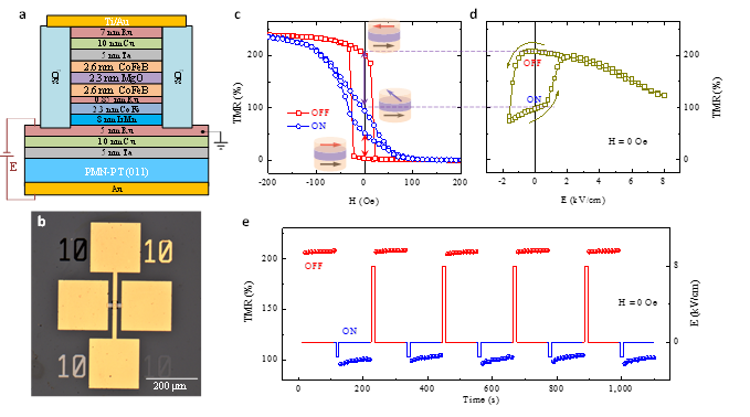
(a) Schematic of the MTJ device structure deposited on PMN-PT (011). Voltage was exerted on the FE substrate to avoid devastating the MTJs. (b) Top view of a typical MTJ device taken with an optical microscope. The numbers are used for mark. (c) TMR curves at E = 0 kV/cm for the OFF and ON cases, respectively. The insets illustrate the relative magnetization alignment at zero magnetic field. (d) Dependence of TMR ratio on electric field under zero magnetic field. The two distinctive resistance states at E = 0 kV/cm indicate nonvolatile and reversible electrical manipulation of TMR. (e) Repeatable bistable TMR states modulated by asymmetric electric-field pulses in the absence of a bias magnetic field. Before measurements in (d) and (e), the device was initialized to a high TMR state with the antiparallel magnetization configuration after a magnetic field of –300 Oe.
b. Electronic and Magnonic Spin-current in Antiferromagnetic (AFM) Layers
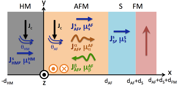
We investigate the spin-orbit torque in a Ta/IrMn/Cu/NiFe multilayer heterostructure and relate it to spin current transmission through the IrMn layer. We identify several spin current transport regimes as a function of temperature and thickness of the IrMn layer. To interpret this experiment, we developed a drift-diffusion model accounting for both electron and magnon transport in the heterostructures.